Micro Robot miBotTM
High precision robots for microscopes
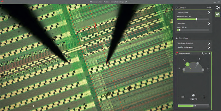
We offer high-precision robotic solutions to interact with and characterize samples down to the nanometer scale. Based on a unique motion technology, positioning probes with our robots and maintaining stable electrical contacts has never been so easy. The high modularity of our solutions provides considerable flexibility for deep integration with a variety of microscopy and test equipment, enabling efficient measurement workflows.
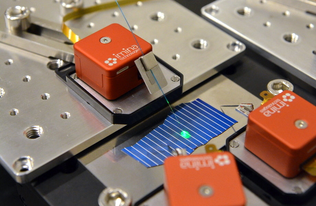
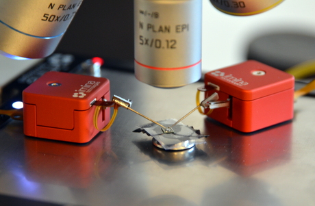
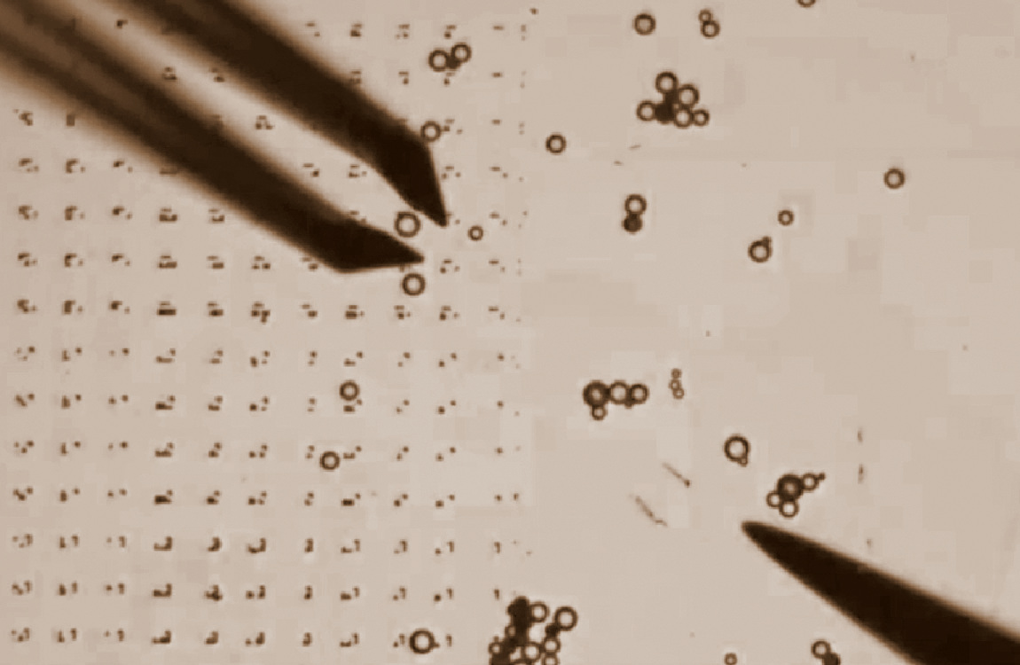
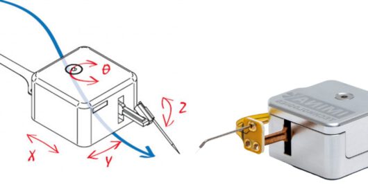
The Imina Technologies miBot™ is, an extremely versatile and intuitive to use piezo-based manipulator. In combination with various third party instruments, it is used to precisely position probe tips on electronic devices and MEMS, or to handle and characterize properties of nanoparticles and biological samples.
- 4 Degrees of Freedom
- Large Travel Range of Several cm
- Resolution Down to nm
- High Stability
- Intuitive to Control
Our Offering is divided into 2 Product Lines – MICRO and NANO – with a High Level of Upgradability between each other that adapt to your Equipment, Samples, and Experimental Requirements.
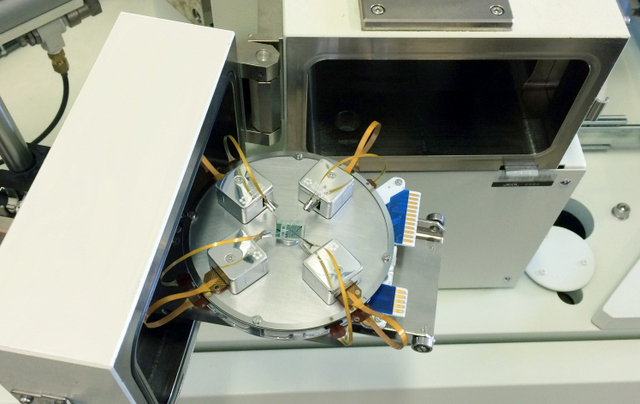
NANO Product Line
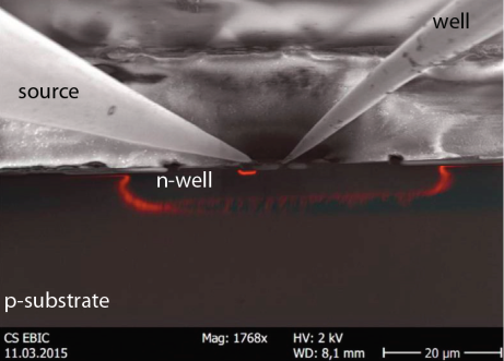
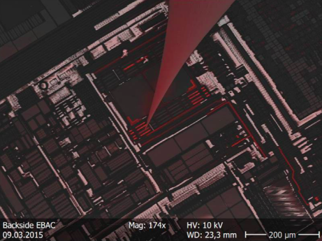
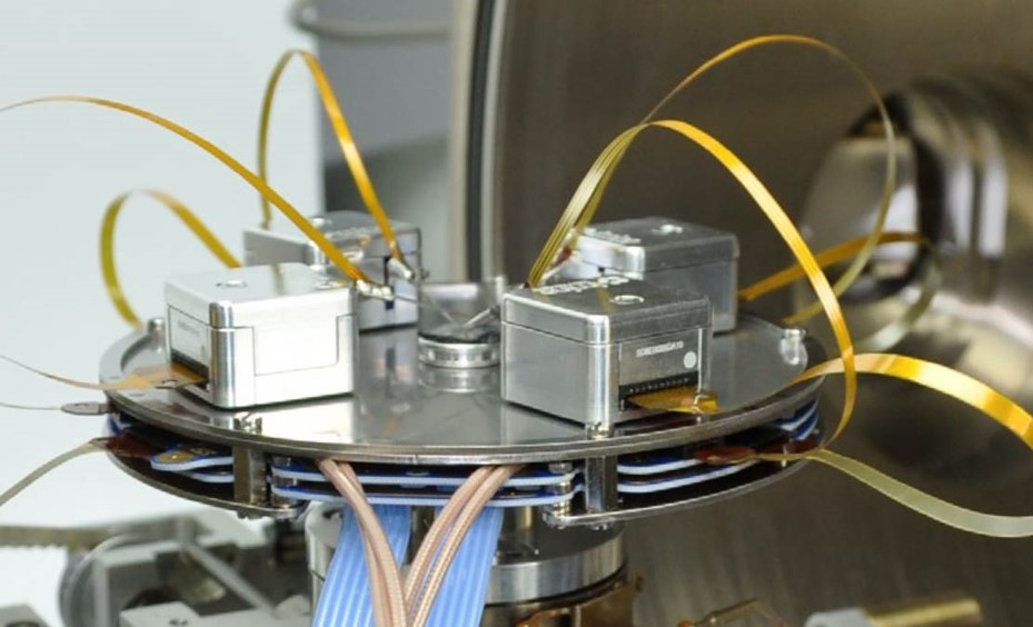
In-situ Nanoprobing and Electrical Failure Analysis (EFA) Solutions for SEM,FIB or Dual Beam.
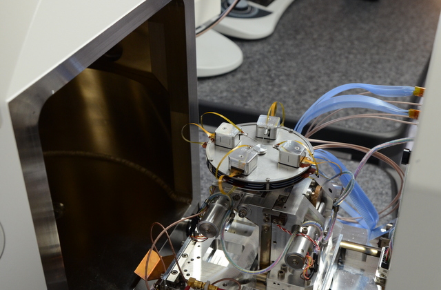
The Positioning Resolution is < 1 nm. Removable Platforms easily (in Minutes) are mounted on the Sample Position Stage of most SEM Models. The Platforms can be used with up to 8 miBot™ Mobile Nanoprobers.
The Solutions are compatible with Advanced Microscopes, using short Working Distances, Tilted Angles, and Magnetic Immersion Mode.
EFA Applications like EBAC/RCI, EBIC, EBIRCh are supported.
Our Precisio™ Software provides an Integrated Workflow to allow Positioning oft the Nanoprobes, running Electrical Test Measurements, and to Support Processing and Reporting.
New: Robot NANO+ for safer and faster probe landing
15um fine motion range in Z (arm/probe)
Faster and easier probe landing (2 to 4 times) on sample contact area
Safer experiments, less sample/probe damage
Available as an Upgrade for existing NANO – miBots
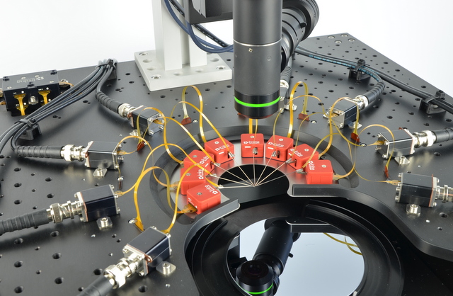
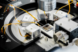
MICRO Product Line
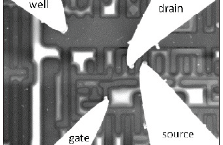
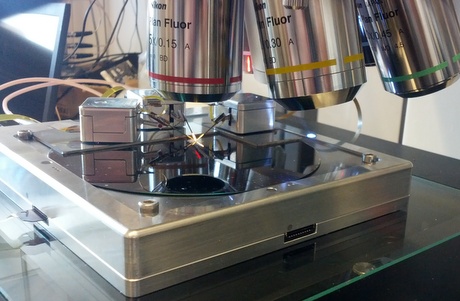
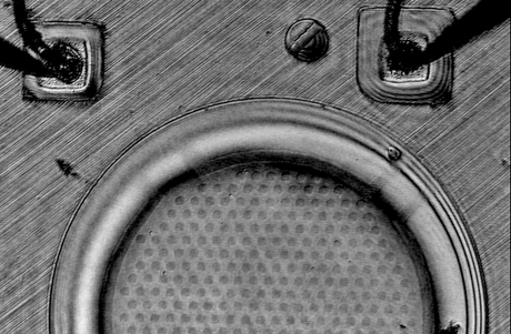
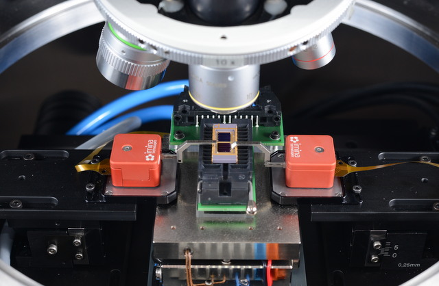
Precisely Position Probes, and physically interact with Samples, using miBots™ integrated to Optical Microscopes, Probe Stations and Inspection Tools.
The Positioning Resolution is < 100 nm. Different Platforms adapt to the available Space and Experimental Needs, and can hold up to 8 miBot™ Mobile Robots.
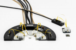
Stand-Alone Probe Stations for either small Probes or Wafers can allow Semi-Automatic Operation.
Microprobing Platform Kits integrate to existing upright or inverted Optical Microscopes, Probe Stations, Semiconductor Inspection Tools, AFMs or Glove Boxes/Environmental Chambers.
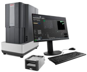
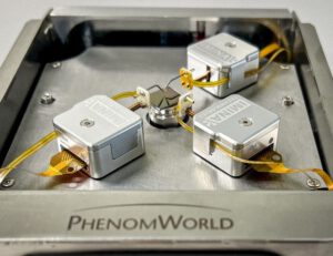
TFS Phenom Integration
The Phenom electron microscopes are not only smaller, simpler and cheaper than a large device, they are also much faster thanks to the low vacuum in the sample chamber and do not require any coating of non-conductive surfaces.
Desktop SEM devices offer greater ease of use and democratize SEM technology. Additionally, they offer the added benefit of a smaller frame size. While traditional standalone SEM devices may require a dedicated space or setup, desktop devices are far more robust.
Some users have even taken their desktop SEMs out of the lab and are offering on-site analysis using electron microscopy through mobile labs.
In-situ desktop SEM electrical probing and manipulation
Available with model Phenom XL G2
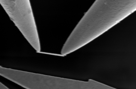
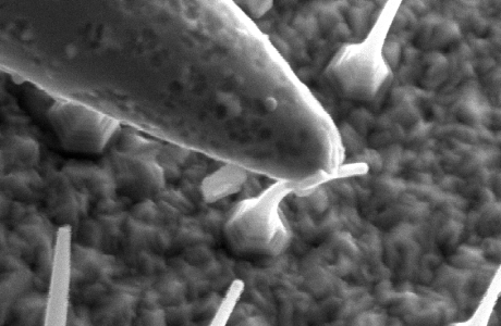
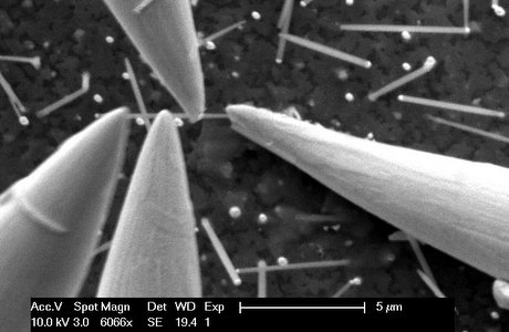
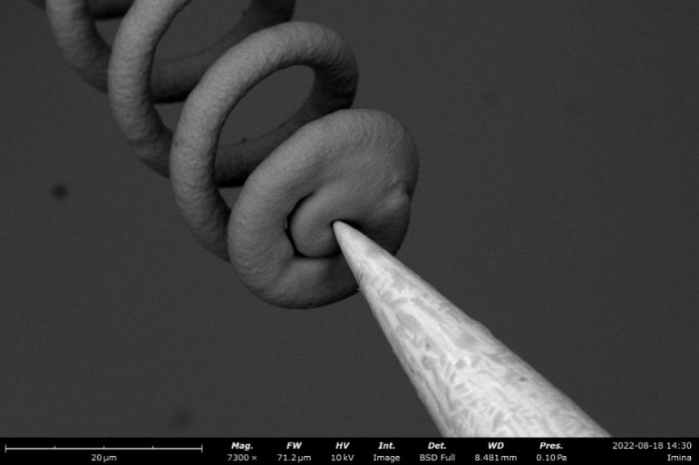
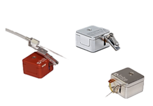
Probes and Sensors
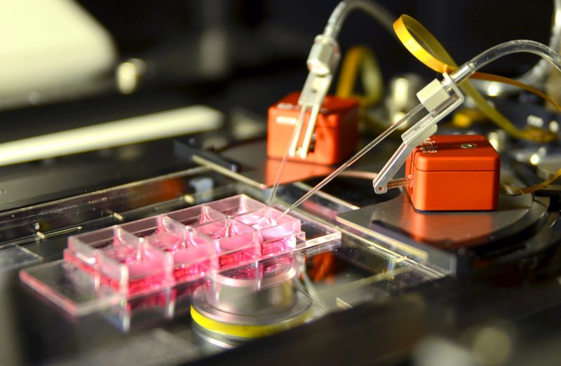
Extend the use of your miBot™ to various Types of Applications thanks to its Compatibility with several Tools and Sensors. In Fact, the miBot™ is equipped with a Proprietary Tool Holder Mechanism that makes the Exchange or Replacement of Tools fast and convenient. In Minutes, turn the miBot™ from an Electric Probe or Manipulator to an Optical Fiber Positioner or Micropipette Positioner. Special Tool Holders for other Tools are available on Request ( e.g. MEMS, mulitiprobes, miniforks, AFM probes).
Applications:
|
Typical Samples:
|