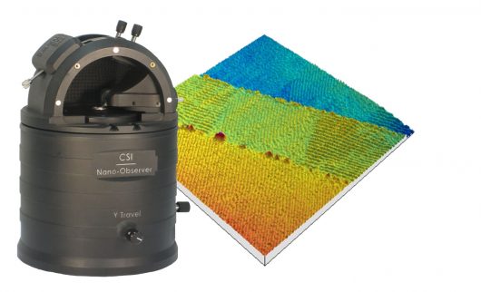
CSI Nano-Observer
CSI Nano-Observer Multiple-Mode AFM
The Nano-Observer AFM microscope is a flexible and powerful AFM platform for various operation modes and measurement conditions.
It´s development is the result of many years of collaboration with different AFM players and laboratories.
The result is a clever combination of analog and digital electronics, incorporating premium components to offer the lowest noise and best accuracy on a robust and flexible instrument.
The Nano-Observer uses an advanced flat scanning stage to avoid well known defects of the piezoelectric tube scanner such as bow, X-Y crosstalk etc..
A low noise feedback control delivers reliable and high performance.
Easy to use and intuitive operation
Pre-aligning tip holders avoid time consuming laser alignment
A top and side view video microscope with lateral illumination ensures a perfect optical control for tip approach and sample navigation
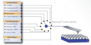
8 electrical contacts to the tip allow the operation in different modes with one and the same tip
The intuitive Nanosolution software allows the simple switching between pre-configured measurement-modes without adding modules or connections
Multiple Modes
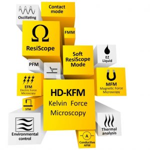
The Nano-Observer platform is based on a modular design. In addition to the standard configuration that allows the operation of all topography modes, the AFM can be upgrade with advanced electrical modes for measuring electrical fields, sample resistivity, doping concentration, piezoelectric properties but also for magnetic properties in magnetic field generators, measurements in special gas atmospheres, liquid or variable temperatures:
High Definition Kelvin Force Microscopy
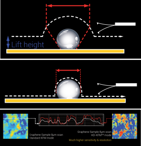
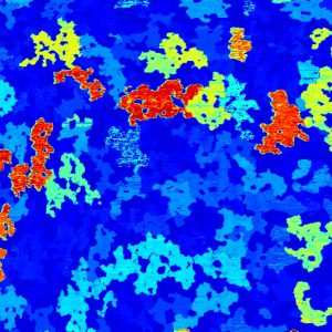
Kelvin Force Microscopy (KFM) allows to determin the surface potentials between the AFM tip and the surface with high lateral resolution which can be related to material properties like the work function or the bandgap.
Standard-KFM is based on a dual pass technology (Lift Mode) with a typical tip to sample distance of 10-50 nm, when the surface potential is measured.
High Definition Kelvin Force Microscopy (HD-KFM) is much more sensitive and provides a much higher lateral resolution as the surface potential is acquired simultaneously with the topography by lock-in technique.
ResiScopeTM and Soft ResiScope
Advanced Conductive Nano-Characterization
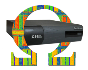
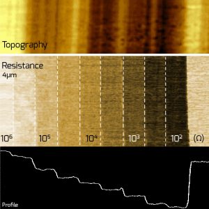
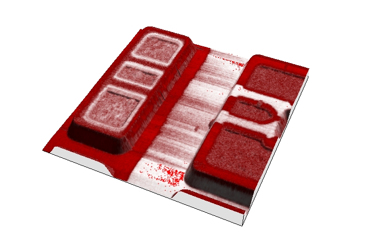
The ResiScope is the most advanced module for conductive measurements that enables conductivity measurements over 10 decades (from 100 fA to 1 mA) within one image.
Surfaces with both, highly conductive and insulating domains can be mapped overcoming undesired side-effects like probe-induced local oxidation, bimetallic effects or melting of the conductive coating.
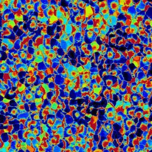
It can be combined with several dynamic modes as MFM/EFM or KFM providing several signal channels with the same tip on the same sample area.
The Soft ResiScope enables the conductivity measurement also for the Intermittent Contact Mode.
So even for fragile and soft surfaces, conductivity maps can be acquired that would never be measurable with Contact Conductive AFM techniques
Scanning Microwave Impedance Microscopy
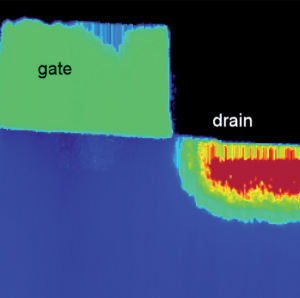
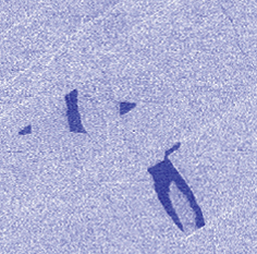
Scanning Microwave Impedance Microscopy (sMIM) is a new AFM imaging mode providing the carrier concentration and carrier type (n or p) in high quality images with a resolution of better than 50 nm.
The core of sMIM technology is utilizing 3GHz microwave reflections from a nm-scale sample region directly under the very small spatial region of a sMIM probe tip.
By analyzing the sample response, the local sample properties: ε,σ,& μ can be determined.
This method is compatible with a wide range of materials: dielectrics, insulators, semiconductors, and metals.
Unlike other conventional electrical AFM modes, sMIM can simultaneously image these different materials classes without multiple settings or measurements.
Magnetic Lateral Field Module
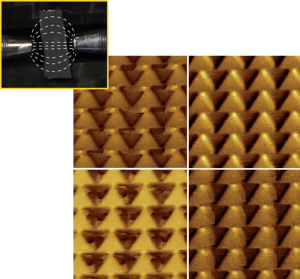
Magnetic Lateral Field Module (MLFM) allows Magnetic Force Microscopy (MFM) measurements in a controllable external magnetic field. A possible application is for example the mapping of magnetic domain behavior in dependence of the external field strength.
Environmental control and optical access
The Nano-Observer is designed to offer environmental control (gas, humidity…). It is compatible to all electrical modes that often require dry and oxygen-free conditions.
In addition the sample temperature can be controlled from ambient to 200°C to investigate temperature-dependent surface property changes.
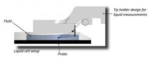
Also a plug and play Liquid Cell is available. It enables liquid scanning without any additional adjustments or laser prealignment.
The compact design of the Nano-Observer further easily enables the integration into an optical analysis setup like Raman for example.
Application Fields:
- Semiconductors
- Metals
- Nanotechnologies
- Photovoltaic
- Thin film & coating
- Polymers
- DNA
- Cell
- Proteins
